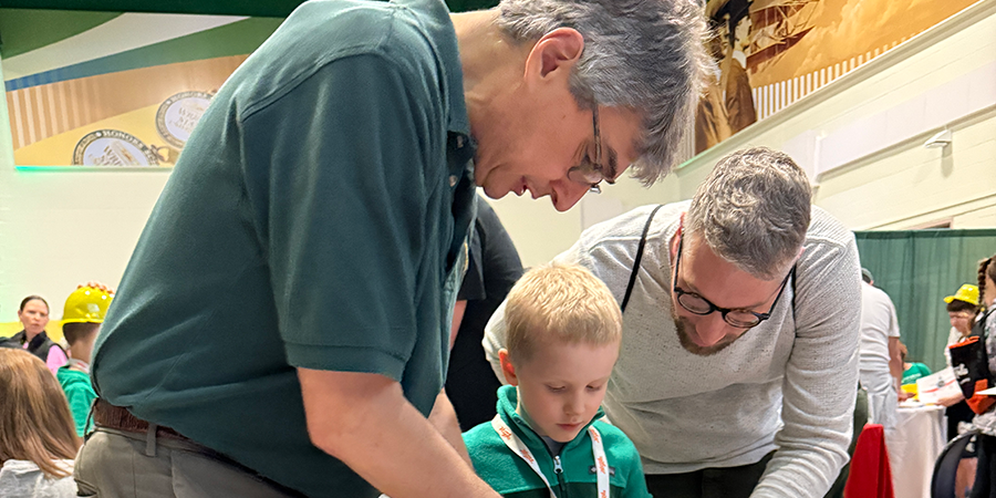

Registration for CVD 2026 Has Reached Capacity; Waitlist Available
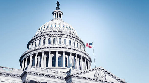
IEEE-USA’s annual Congressional Visits Day (CVD) will take place 17-18 March 2026 in Washington, DC. CVD gives IEEE Members in the United States the opportunity to meet with their Congressional representatives and key staff to raise awareness of engineering and technology’s long-term importance to the nation, and to discuss technically sound policy solutions. Registration has reached full capacity, after but you may join the waitlist and we will contact you if a space opens.
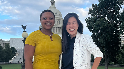
Apply by 23 February for 2026-2027 IEEE-USA Congressional Electric Grid Policy Fellowship
The IEEE-USA Congressional Electric Grid Policy Fellowship seeks to augment the capabilities of congressional staff by selecting and placing qualified Fellows with relevant technical expertise in offices or on committees actively working on grid policy. Deadline to apply is 23 February 2026.
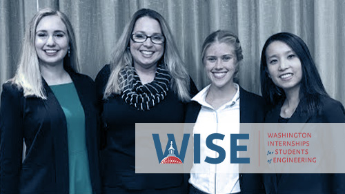
Spend Next Summer in Washington, DC:
Apply Now for WISE 2026!
Qualified IEEE Student Members can spend next summer in Washington DC learning how government officials make decisions on complex technological issues, and how engineers and scientists can contribute to the process. The deadline to apply for Summer 2026 is 1 March 2026.
IEEE-USA 168体彩一分钟极速赛车赛果历史数据、赛车在线预测跟单计划+赛果直播 Calendar
IEEE-USA hosts dozens of career and policy-oriented webinars, and also serves as co-sponsors or technical co-sponsors of technical and professional conferences whose proposed programming includes career development and/or public policy content aligned with IEEE-USA’s mission and areas of expertise.
Important Dates
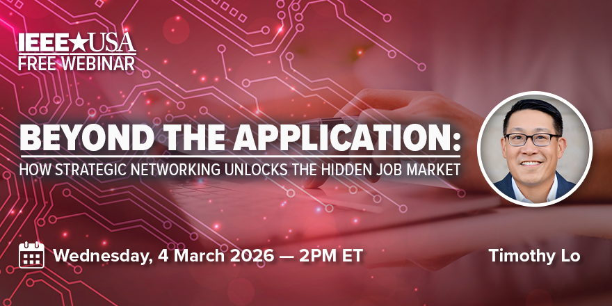
4 March 2026 @ 2:00 pm - 3:00 pm
Livestream Webinar
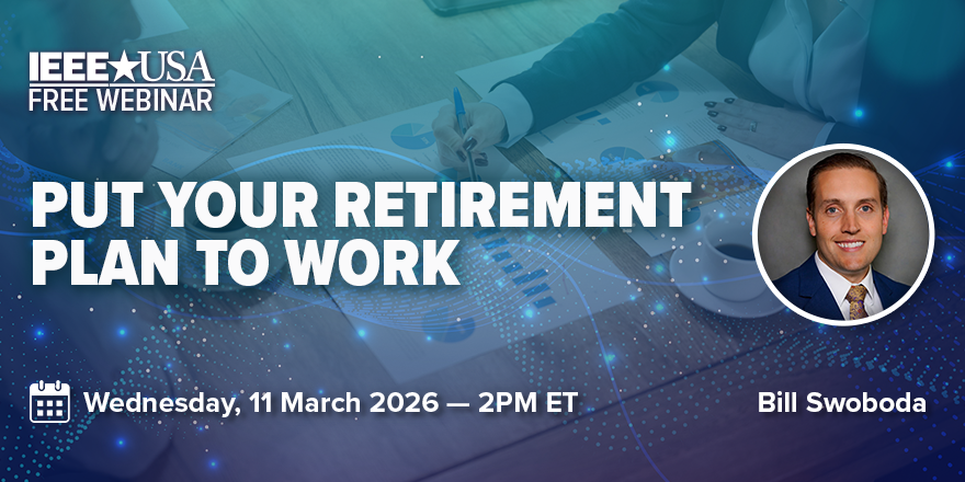
11 March 2026 @ 2:00 pm - 3:00 pm
Livestream Webinar
IEEE-USA 168极速赛车一分钟开奖结果记录体彩官网 is my Competitive Edge
IEEE-USA’s 2026最新极速赛车的赛果历史记录、168赛车预测计划+全国统一开奖网、极速一分钟赛车官方开奖官网入口 series of short, high-quality videos profiles a handful of rock stars from the profession, and highlights what their IEEE membership means to them personally and professionally. The common thread that emerged during the production of the videos is that “IEEE-USA is my Competitive Edge.”