We are living in the era of heterogenous integration driven by fast, efficient and big data computing resources at our fingertips. The mega-monolithic silicon chip is a thing of the past, replaced with 3D heterogenous integration of chiplets onto a platform made of an organic build-up substrate. Volume manufacturers of build-up substrates are entirely based in Asia, leaving a desert in the US. Volume build-up substrates used by major IDMs are manufactured in Asian countries including Taiwan, Japan and China.
However, there are multiple activities starting up in the US, and this is why a gathering of the US players is important. This symposium is geared for all those involved in the supply chain of build-up substrates in the US, as well as users. As the US Congress debates H.R. 3249, the Protecting Circuit Boards and Substrates (PCBS) Act, this Symposium is an opportunity for all build-up substrate players to meet, network and cohesively work with funding agencies who will be invited to this symposium to focus on onshoring build-up substrate production and utilization.
Sessions:
— Substrate Manufacturing and Onshoring
— Materials for Substrates
— Emerging Substrate Technologies
— Panel Equipment and Technologies for Substrates
— Inspection and Testing
|
… plus two panels:
— Substrate End Users
— Onshoring and Startups

PLAN TO ATTEND!
|
Confirmed Speakers at BUSS:
 Wafer Level Substrates – An Emerging New Technology Wafer Level Substrates – An Emerging New Technology
Steven Verhaverbeke, Applied Materials |
|
 Advanced X64 UCIe Interface Implementation on a Substrate Advanced X64 UCIe Interface Implementation on a Substrate
Farhang Yazdani, Broadpak |
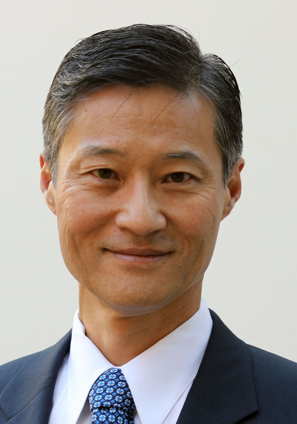  Chiplet Integration on Organic Buildup with Silicon Interconnect Fabric Chiplet Integration on Organic Buildup with Silicon Interconnect Fabric
Vineeth Harish, UCLA, and Prof. Ken Yang, UCLA |
|
 The Future of AI and HPC Substrates: A Breakthrough Interconnect Technology The Future of AI and HPC Substrates: A Breakthrough Interconnect Technology
Rozalia Beica, LQDX |
 Substrate Materials for Advanced Packaging Substrate Materials for Advanced Packaging
Masato Fukui, Resonac America |
|
  NAPMP Plans and Advanced Substrate Onshoring NAPMP Plans and Advanced Substrate Onshoring
Dan Berger, NIST, and Subramanian Iyer, UCLA |
 Advanced Packaging Metallization: Substrate Interaction with Catalyst and Electroless Deposition of Copper Advanced Packaging Metallization: Substrate Interaction with Catalyst and Electroless Deposition of Copper
Purnima Narayanan, Yield Engineering Systems |
|
 QCW CO2 Laser Drilling for FCBGA Applications QCW CO2 Laser Drilling for FCBGA Applications
Kyle Baker, MKS Instruments |
 Systems Solutions for Advanced IC Substrate Manufacturing Systems Solutions for Advanced IC Substrate Manufacturing
Frank Bruening, MSD-Atotech |
|
 Enhancing Water Quality and Environmental Sustainability in ICS Manufacturing with Zero Liquid Discharge (ZLD) Enhancing Water Quality and Environmental Sustainability in ICS Manufacturing with Zero Liquid Discharge (ZLD)
Gustavo Ramos, GreenSource Engineering |
 The Latest Vacuum Lamination Challenges and Technology Development The Latest Vacuum Lamination Challenges and Technology Development
Takuma Yoshikawa, Nikko Materials |
|
 Advanced Insulating Material for Next-Generation Packaging Advanced Insulating Material for Next-Generation Packaging
Yoshio Nishimura, R&D Group manager, Ajinomoto Co., Inc.
|
 2.xD Integrated Substrate Solutions for High-Performance Computing 2.xD Integrated Substrate Solutions for High-Performance Computing
Dr. Dyi-Chung Hu, SiPlus Co. |
|
 Advanced Metrology for High-Density Substrates Advanced Metrology for High-Density Substrates
Dr. Robert Bishop, Beltronics Inc.
|
 USA Landscape for Substrate Manufacturing USA Landscape for Substrate Manufacturing
Venky Sundaram, 3D System Scaling |
|
 Advanced Insulating Material for Next-Generation Packaging Advanced Insulating Material for Next-Generation Packaging
Yoshio Nishimura, R&D Group manager, Ajinomoto Co., Inc.
|
 Packaging Substrate Solutions for Advanced Packaging Requirements Packaging Substrate Solutions for Advanced Packaging Requirements
Dr. Sung Jin Kim, Absolics |
|
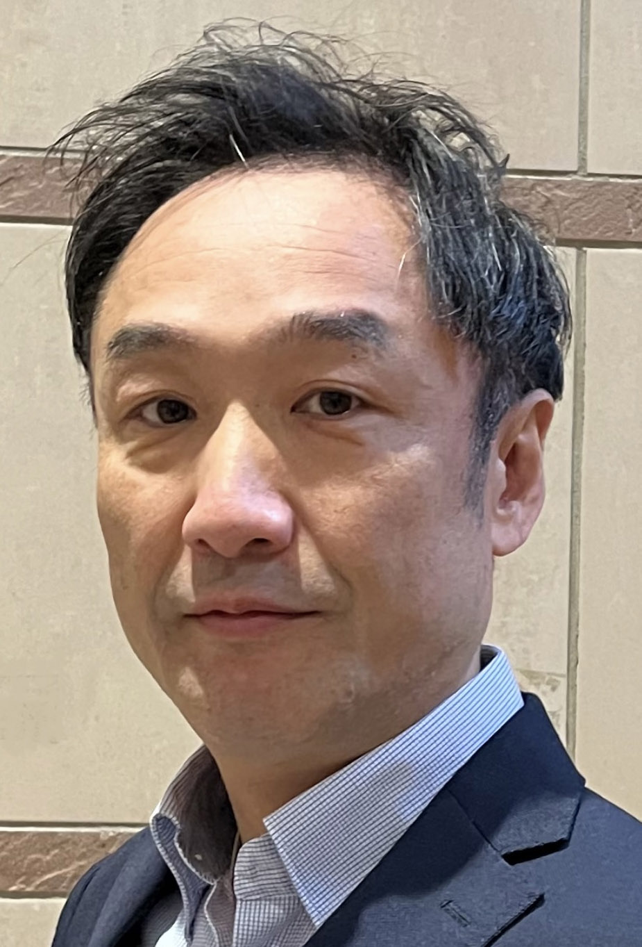 Taiyo’s Photo-Dielectric for High Density Substrate Applications Taiyo’s Photo-Dielectric for High Density Substrate Applications
Yuta Ogawa, Taiyo Ink |
Download the Advance Program
|
|
|
ORGANIZER:
with Orange County Chapter
SPONSORS:


Become a Sponsor!
|



 Wafer Level Substrates – An Emerging New Technology
  Advanced X64 UCIe Interface Implementation on a Substrate
 Chiplet Integration on Organic Buildup with Silicon Interconnect Fabric
  The Future of AI and HPC Substrates: A Breakthrough Interconnect Technology
  Substrate Materials for Advanced Packaging
 NAPMP Plans and Advanced Substrate Onshoring
  Advanced Packaging Metallization: Substrate Interaction with Catalyst and Electroless Deposition of Copper
  QCW CO2 Laser Drilling for FCBGA Applications
  Systems Solutions for Advanced IC Substrate Manufacturing
  Enhancing Water Quality and Environmental Sustainability in ICS Manufacturing with Zero Liquid Discharge (ZLD)
  The Latest Vacuum Lamination Challenges and Technology Development
  Advanced Insulating Material for Next-Generation Packaging
  2.xD Integrated Substrate Solutions for High-Performance Computing
  Advanced Metrology for High-Density Substrates
  USA Landscape for Substrate Manufacturing
  Packaging Substrate Solutions for Advanced Packaging Requirements
  Taiyo’s Photo-Dielectric for High Density Substrate Applications

